Industrial Problem-Solving through Domain-Specific Models and Agentic AI: A Semiconductor Manufacturing Case Study
The semiconductor industry is at a crossroads, facing a critical shortage of specialized expertise for establishing and operating cutting-edge manufacturing facilities. This gap impacts project timelines, drives up costs, and limits innovation in a growing field ever more complex.
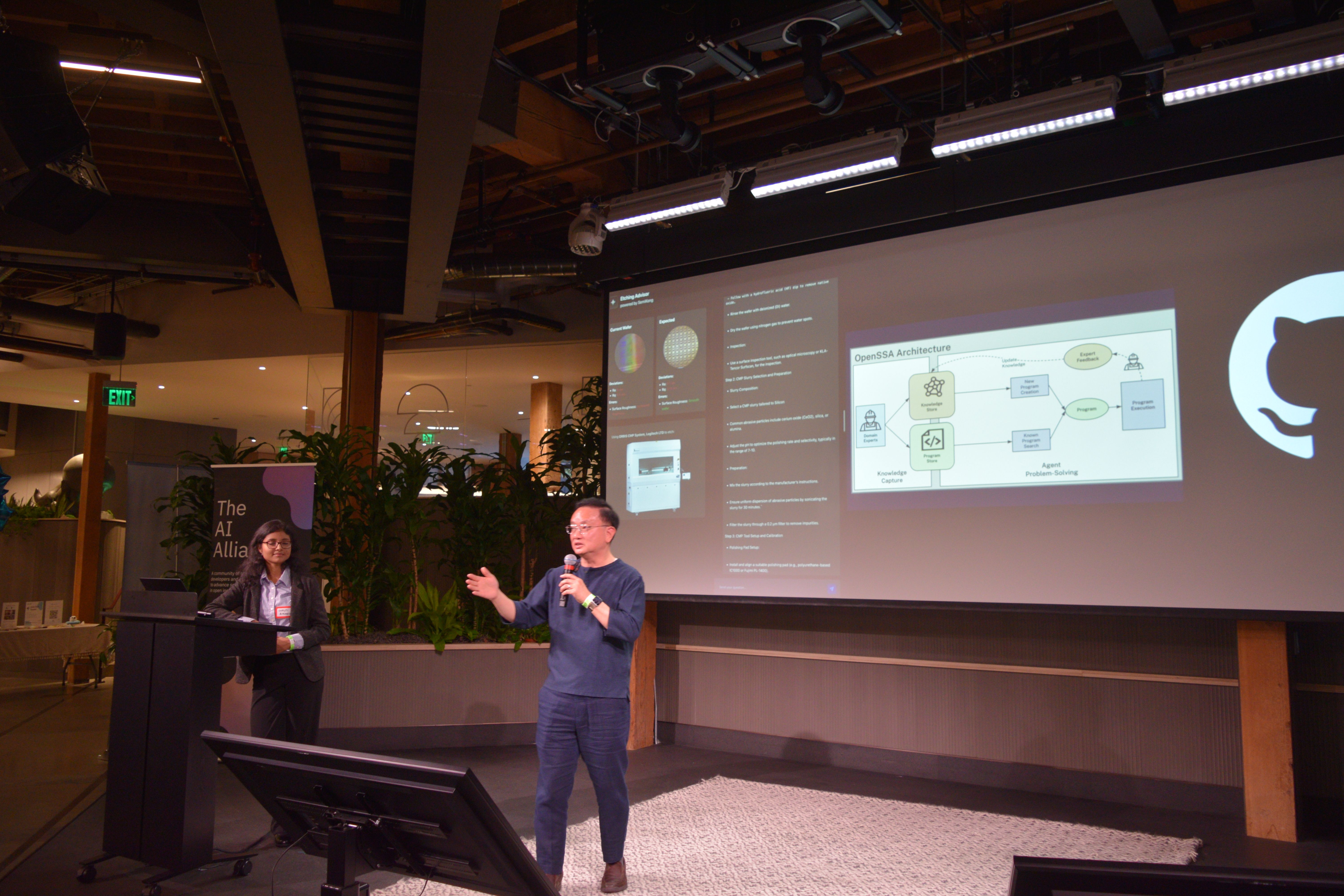
During the recent SF Unstructured Data Meetup, industry experts Christopher Nguyen and Shruti Raghavan from Aitomatic explored how AI can bridge this expertise gap. Their insights revealed how domain-specific models and agentic AI systems can capture, share, and apply specialized knowledge, offering a way forward for the industry. This article will recap their key points and discuss how Milvus, the most popular vector database, can be used in the industrial AI domain. Let’s begin by looking at a real-world example of a company experiencing an expertise challenge. Watch the recap of the talk on YouTube.
The Expertise Challenge: A Tale of Two Projects
Christopher illustrated the expertise shortage by contrasting the outcomes of two similar projects by Taiwan Semiconductor Manufacturing Company (TSMC). Both projects use identical technology and have comparable financial backing, yet their progress differs significantly. In Kyushu, Japan, the facility under construction is progressing well. On the other hand, the one in Phoenix, Arizona, is encountering difficulties due to a shortage of local expertise.
This disparity highlights how the availability of specialized knowledge and experience can significantly influence project outcomes, even when technological and financial resources are similar. This contrast highlights a key question: how can the semiconductor industry mitigate such expertise disparities, and could any AI-driven solutions provide a scalable answer?
Limitations of General-Purpose AI in Specialized Industries
General-purpose large language models (LLMs) have demonstrated capabilities across various domains but often fall short in specialized industrial applications. In semiconductor manufacturing, the required knowledge extends beyond the scope of these general models.
The output of general LLMs in specialized contexts is comparable to that of a recent graduate—possessing broad knowledge but lacking a seasoned professional's deep, experiential expertise. This limitation becomes evident when dealing with complex manufacturing processes that require nuanced understanding and decision-making based on years of hands-on experience.
For instance, semiconductor manufacturing processes like photolithography (creating circuit patterns on silicon wafers), etching (selectively removing materials from a wafer's surface), and chemical mechanical planarization (CMP, flattening and polishing the wafer surface) require not just theoretical knowledge, but an understanding of how various parameters interact in real-world scenarios.
This is where domain-specific models become critical in bridging the gap between general AI capabilities and the nuanced needs of semiconductor manufacturing.
Domain-Specific Language Models for Semiconductor Manufacturing
To address the limitations of general-purpose LLMs, industry-specific models are being developed for the semiconductor domain. SemiKong, an open-source project from the AI Alliance specific to the semiconductor domain, is an example of such a model. These specialized models aim to incorporate domain-specific knowledge to address the unique challenges faced by the semiconductor industry.
The features of SemiKong include:
Industry-specific training data: The model is trained on semiconductor-related texts, including research papers, technical documents, and industry reports.
Domain-specific pre-training: The model uses pre-training approaches that leverage semiconductor industry knowledge.
Performance on industry-relevant tasks: SemiKong is benchmarked against general-purpose LLMs on semiconductor-specific tasks.
Foundation for proprietary models: Organizations can use SemiKong as a starting point to build models tailored to their specific manufacturing processes and challenges.
SemiKong builds upon open-source foundations, allowing integration with existing AI workflows and tools used in the industry.
Advanced AI Architectures for Industrial Applications
Building on the specialized capabilities of models like SemiKong, Aitomatic has developed an Open Small Specialist Agents (OpenSSA) architecture. This approach leverages the deep industry knowledge embedded in SemiKong to create agentic AI systems capable of complex decision-making in semiconductor manufacturing, extending beyond simple information retrieval to active problem-solving.
OpenSSA operates through several interconnected components, that enable efficient knowledge management, problem-solving, and expert feedback integration:
Knowledge CaptureThe foundation of the system starts with capturing expert knowledge from domain specialists, such as process engineers and equipment experts. This expert input is stored in two essential repositories:
Knowledge Store: It holds detailed insights provided by these specialists, which the system can draw upon when addressing problems.
Program Store: Alongside the knowledge store, this repository contains reusable programs or solution templates designed to solve recurring manufacturing challenges.
Together, these repositories form the backbone of the system's problem-solving capabilities, providing a rich source of industry-specific information and proven solutions.
Agent Problem-SolvingBuilding on the captured knowledge, the system’s AI agents can tackle both new and familiar problems. When faced with a challenge, it can either create a new problem formulation by referencing information from the knowledge store or search for known solutions in the program store when a similar problem has been encountered before.
By seamlessly integrating knowledge with problem recognition, the system develops strategies tailored to each situation, ensuring effective solutions are always within reach.
Program ExecutionOnce a solution strategy is formulated, whether it’s a new approach or a known one, the system moves to execution. This is where it interfaces with real-world manufacturing environments, such as Manufacturing Execution Systems (MES), to implement these solutions directly. The execution phase marks the culmination of the system’s problem-solving process.
Expert FeedbackAfter the AI executes the solution, human experts review the outcomes and provide critical feedback. This feedback loop ensures that the system remains grounded in real-world expertise, allowing it to learn from each execution and refine its future strategies. Expert input improves the AI's understanding of evolving manufacturing challenges.
Knowledge UpdatesExpert feedback is then used to update both the knowledge and program stores, ensuring that the AI system continuously improves.
The OpenSSA architecture aims to create AI agents that can leverage both broad language model capabilities and specific domain expertise to solve complex problems in semiconductor manufacturing. For example, an AI agent might assist in optimizing a plasma etching process by considering multiple factors such as gas flow rates, chamber pressure, and RF power settings, drawing on its knowledge base and problem-solving capabilities to suggest optimal parameters.
To see the AI agent in action, watch this video.
Hierarchical Task Planning and Iterative Decision-Making
AI agents developed using architectures like OpenSSA employ sophisticated problem-solving strategies. Robert and Shruti showcased how AI can approach problem-solving through hierarchical task planning and iterative decision-making, critical for adapting to the variable conditions of semiconductor manufacturing.
The AI agent's problem-solving approach consists of two key aspects:
Hierarchical Task Planning
Hierarchical task planning involves breaking down complex tasks into smaller, manageable subtasks. This approach creates a tree-like structure of tasks and subtasks, allowing the AI to manage intricate manufacturing processes efficiently.
For example, when optimizing a chemical vapor deposition (CVD) process, the AI breaks it down into the following subtasks:
Adjusting gas flow rates
Controlling chamber temperature
Optimizing deposition time
Monitoring film thickness
Each of these subtasks can be further divided if necessary, creating a multi-level hierarchy of tasks. This structure enables the AI to tackle complex problems systematically, ensuring that all aspects of a process are addressed.
Iterative Decision-Making (OODA Loop)
The AI employs an iterative decision-making process known as the OODA loop (Observe, Orient, Decide, Act) to guide its actions at each level of the task hierarchy. This continuous cycle allows the AI to adapt to changing conditions in real-time:
Observe: The AI gathers data from sensors and manufacturing systems, collecting relevant information about the current state of the process.
Orient: It analyzes the collected data in the context of the current manufacturing process, considering historical data and known parameters.
Decide: Based on the analysis, the AI chooses the best action to take, weighing various options and their potential outcomes.
Act: The chosen action is implemented, affecting the manufacturing process.
This cycle repeats continuously, allowing the AI to respond dynamically to changes in the manufacturing environment. For instance, if the AI detects an unexpected change in gas flow rates during the CVD process, it can quickly adjust other parameters to maintain optimal deposition conditions.
This combination of hierarchical planning and iterative reasoning enables the AI to handle complex, multi-faceted problems in industrial settings effectively. It allows for both high-level strategic planning and rapid, tactical decision-making at the operational level. This forms the backbone of practical applications, such as optimizing semiconductor manufacturing processes like plasma etching.
Practical Application: AI-Assisted Etching Process Optimization
A practical application of these AI approaches is in etching process optimization. Etching is a critical step in semiconductor manufacturing where specific areas of a silicon wafer are removed to create the intricate patterns necessary for chip functionality. Aitomatic has developed systems that combine domain-specific language models with the OpenSSA architecture to enhance semiconductor manufacturing capabilities.
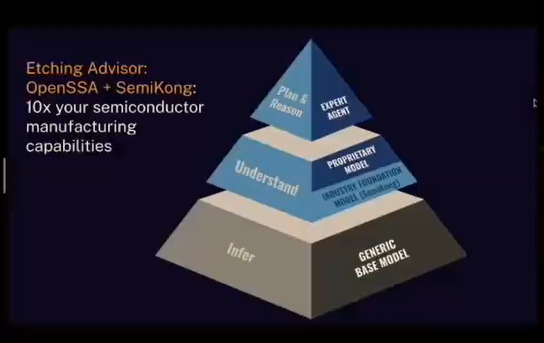 Figure 1- Etching Advisor Architecture.png
Figure 1: Etching Advisor Architecture
Let’s look at what is happening in the layered architecture for an AI-assisted etching optimization system:
Base Layer: This foundation layer provides basic inference capabilities and general language understanding. It can process natural language queries from engineers and interpret basic manufacturing data.
Middle Layer: This layer offers comprehension of domain-specific concepts and integrates company-specific knowledge. It understands specialized terms like aspect ratio (the ratio of depth to width in an etched feature) or selectivity (the ability to etch one material faster than another) and can incorporate a company's proprietary process recipes.
Top Layer: This layer delivers advanced problem-solving capabilities and encapsulates expert-level knowledge in semiconductor etching. It can suggest complex multi-step etching strategies, predict potential issues like mask erosion or etch stop, and recommend preventive measures.
Each layer builds upon the capabilities of the ones below it, allowing the system to provide detailed recommendations for complex etching processes by combining general knowledge with specialized expertise. For instance, when optimizing a deep trench etch for a memory chip, the system might suggest adjusting the gas mixture to improve sidewall passivation, recommend a specific power cycling strategy to prevent notching, and propose a post-etch treatment to remove residues.
For these AI systems to function efficiently, they require robust data management solutions. This is where Milvus, a high-performance vector database, plays a crucial role by enabling the effective retrieval and storage of complex manufacturing data for various purposes.
The Role of Milvus in Industrial AI
Milvus plays a crucial role in enabling advanced AI applications in industrial settings, particularly in semiconductor manufacturing. Its features and capabilities make it well-suited for handling the complex data and retrieval needs of modern AI systems, especially when implementing Retrieval-Augmented Generation (RAG) with domain-specific language models like SemiKong.
Key Features of Milvus for Industrial Applications
Multi-tenancy: Milvus allows multiple users or applications to work on the same system without interfering with each other. In semiconductor manufacturing, this enables different teams or production lines to have secure, isolated access to their specific data while sharing the same infrastructure.
Hardware-accelerated Compute: Optimized for various hardware environments (including AVX512, Neon for SIMD, and GPU acceleration), Milvus delivers fast processing for resource-intensive tasks. This is particularly valuable for real-time analysis of complex manufacturing data or AI model inference for process optimization.
Language and API Support: With support for Python, Java, Golang, NodeJS, and more, Milvus integrates seamlessly with various development environments and existing industrial software ecosystems.
Scalable and Elastic Architecture: As semiconductor manufacturing data grows over time, Milvus automatically scales to meet demand, ensuring consistent performance even as historical process data accumulates.
Diverse Index Support: Milvus supports multiple index types (e.g., HNSW, PQ, Binary, DiskANN), allowing flexibility in how manufacturing data is stored and searched. This enables efficient retrieval of relevant information for specific manufacturing scenarios.
Tunable Consistency: The ability to adjust consistency levels allows semiconductor manufacturers to balance between query performance and data accuracy based on the specific needs of different manufacturing processes or quality control requirements.
Milvus in RAG Systems for Semiconductor Manufacturing
When implementing a RAG system using Milvus and a domain-specific LLM like SemiKong for semiconductor manufacturing, the process looks like this:
Knowledge Base Creation:
Vector embeddings are created from technical documents, research papers, and manufacturing logs.
These are stored in Milvus, leveraging its diverse index support for optimal storage and retrieval.
Query Processing:
An engineer inputs a problem description (e.g., unexpected etch rate variations).
The query is converted to a vector representation.
Retrieval:
Milvus performs a similarity search using its hardware-accelerated computing capabilities.
It employs advanced search methods (e.g., top-K ANN, range ANN, filtered searches) to find the most relevant past cases or documents.
Multi-tenancy ensures that only authorized data is accessed.
Augmentation and Generation:
Retrieved information is combined with the original query and fed into the SemiKong LLM.
SemiKong generates a response, combining its semiconductor knowledge with the specific, retrieved information.
Continuous Learning:
- New cases and solutions are added to the Milvus database, leveraging its scalable architecture to maintain performance as the knowledge base grows.
Milvus Technologies for Various Industrial Use Cases
Compute Types: Milvus's optimization for different hardware environments ensures fast processing and cost-effective scalability across various industrial applications.
Search Types: The wide array of search methods allows tailoring search functionality to specific industrial needs, whether it's identifying similar manufacturing defects, matching process parameters, or finding relevant documentation.
Index Types: With 15 indexing types available, Milvus provides options to balance performance, accuracy, and cost for different industrial datasets and query patterns.
Benefits of Milvus in Industrial AI
Enhanced Decision Making: By enabling fast and accurate retrieval of relevant information, Milvus supports data-driven decision-making in complex manufacturing environments.
Improved Efficiency: Hardware acceleration and optimized indexing lead to faster query processing, crucial for real-time industrial applications.
Scalability: As industrial data volumes grow, Milvus's elastic architecture ensures consistent performance without the need for frequent system overhauls.
Flexibility: Support for various programming languages and APIs allows for easy integration with existing industrial systems and workflows.
Data Security: Multi-tenancy features enable secure data handling in shared manufacturing or research environments.
By leveraging Milvus's capabilities in RAG systems with domain-specific LLMs, industries like semiconductor manufacturing can create powerful tools for problem-solving, process optimization, and knowledge preservation. This combination of technologies addresses the challenges of expertise shortages and complex data management in modern industrial settings.
Implications for the Semiconductor Industry and Beyond
The combination of domain-specific language models, agentic AI systems, and vector databases has several implications for the semiconductor industry and other complex manufacturing sectors:
Addressing expertise shortages: These AI systems can capture and disseminate the knowledge of experienced professionals, helping to mitigate the impact of retiring experts and talent shortages. This is crucial in areas like the TSMC project in Arizona, where local semiconductor manufacturing expertise may be limited.
Accelerating innovation in manufacturing processes: By quickly analyzing vast amounts of data and suggesting optimizations, AI can speed up the development and refinement of manufacturing techniques. This could lead to faster adoption of new technologies like extreme ultraviolet (EUV) lithography or 3D chip stacking.
Making high-level expertise more accessible throughout organizations: AI systems can provide expert-level advice to less experienced staff, democratizing knowledge and improving decision-making at all levels of a company.
Enabling the creation of customized, proprietary AI systems: Companies can build on these AI foundations to create systems tailored to their specific manufacturing processes, potentially providing a competitive edge.
Helping companies establish operations in new regions: AI systems can help transfer knowledge and best practices to new facilities, potentially easing the challenges of setting up manufacturing operations in areas with less semiconductor industry experience.
Enhancing process optimization and efficiency: Continuous analysis and optimization of manufacturing processes can lead to improved yields, reduced waste, and higher overall efficiency. This is crucial in an industry where even small improvements in yield can translate to significant cost savings.
Improving predictive maintenance and quality control: AI can predict equipment failures and quality issues before they occur, enabling proactive maintenance and ensuring consistent product quality. This is particularly important in semiconductor manufacturing, where equipment downtime and defects can be extremely costly.
Facilitating faster adaptation to new technologies: As new manufacturing technologies emerge, AI systems can quickly incorporate this knowledge, enabling faster adoption of cutting-edge techniques. This agility is crucial in the fast-paced semiconductor industry, where technological advances occur rapidly.
Conclusion
Robertson and Shruti did a great job at showcasing how domain-specific AI and advanced architectures like OpenSSA can bridge the expertise gap in semiconductor manufacturing. By integrating Milvus, we see how powerful tools for vector data management can enhance AI's ability to deliver precise, real-time solutions in highly specialized industries. Their insights emphasize that with the right technology, even the most complex fields can leverage AI to innovate and optimize processes effectively.
Keep Reading

Expanding Our Global Reach: Zilliz Cloud Launches in Azure Central India
Zilliz Cloud expands to Azure Central India. This new region helps customers meet compliance, reduce latency, and optimize cloud costs when building AI applications.

Introducing Zilliz MCP Server: Natural Language Access to Your Vector Database
Developers can easily manage and query vector databases with natural language via Zilliz MCP Server in AI-native environments.

Vector Databases vs. Hierarchical Databases
Use a vector database for AI-powered similarity search; use a hierarchical database for organizing data in parent-child relationships with efficient top-down access patterns.
